(Actual size = 4.1 x 2.5 inches)
The ECPE-5 PIC Project Board is a self-contained computer that includes
a power supply, dot-matrix displays, discreet LED's, push-button switch
input, digital to analog converter (DAC), digital thermometer, and a
potentiometer for analog control. The project board is based on the
Microchip 16F877 RISC microprocessor. The processor includes on-chip
I/O ports, 10 bit, ADC, timers, UART, and oscillator.
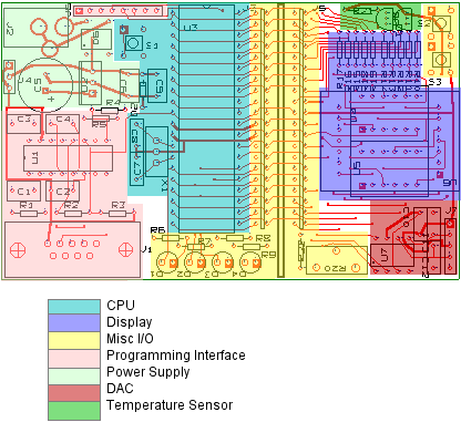
The remainder of this description is divided into sections
along functional lines as indicated in the image above:
CPU,
Dot Matrix Display,
Miscellaneous I/O,
Programming Interface,
Power Supply,
Digital to Analog converter,
and
Temperature Sensor.
D5 protects the board against inverse voltage applied to J4. To make full use of this protection, the external power supply should be fused with a 1amp fuse. Otherwise the power supply will be damaged, or D5 will burn out and the CPU will be damaged.
S1 is the reset switch.
There are two options for the CPU clock. The oscillator, composed of a 20MHz crystal and capacitors C7 and C8, can be replace with a three pin 20MHz ceramic resonator. The frequency will not be as precise or stable with the ceramic resonator, but it should be adequate for the WLoader application. Also note that C7 and C8 are 22pF capacitors, but X1 is cut for a 20pF parallel circuit. The larger capacitance values will skew the crystal frequency slightly, but 20pF capacitors were not readily available in through hole packages, nor could a crystal for a 22pf parallel circuit be found.
U6 is a 1.2 inch high 5x7 dot matrix LED display. It is wired in parallel with a 0.7 inch high 5x7 dot matrix display, U5. U4 is a 0.7 inch high 5x7 dot matrix display that shares row signals with U5 and U6. U6 occupies the same board space as U4 and U5 and therefore can not be installed if either U4 or U5 is present.
The dot matrix LED's are connected to the 16F877 signals as shown below. To turn on a LED, a column signal must be set low and a row signal set high. Resistors R10-R19, connected to the columns, limit the LED current to less than 10mA to protect the 16F877.
Row Signals:
16F877 Signal
LED Display
RD0
Row 1
RD1
Row 2
RD2
Row 3
RD3
Row 4
RD4
Row 5
RD5
Row 6
RD6
Row 7
Column Signals:
16F877 Signal
LED Display
RB0
Col 1, U5/U6
RB1
Col 2, U5/U6
RB2
Col 3, U5/U6
RB3
Col 4, U5/U6
RB4
Col 5, U5/U6
RA0
Col 1, U4
RA1
Col 2, U4
RA2
Col 3, U4
RA3
Col 4, U4
RA4
Col 5, U4
There are four LED's, D1-D4 available for application use. These LEDs are connected to Port C of the CPU. Setting one of the four least significant bits (RC0-RC3) of Port C low will turn on the associated LED. Current through the LEDs is limited to less than 10mA by resistors R6-R9.
There are two switches on the right hand section of the PIC Project
Board.
S2 is connected to the 16F877 RB6 signal and S3 is connected to the RB7
signal. To use the switches the weak-pullup resistors in the 167F877
must be enabled for Port B bits 6 and 7. Note that bits 6 and 7 of Port
B can be configured to generate an interrupt thereby allowing S2 and S3
to be used in an event mode rather than polled.
R20 is a 10k potentiometer connected through the series resistor R22
to signal RE0 of the 16F877. RE0 can be configured as an analog
input (AN5) connected to the 16F877's internal 10 ADC. The signal
from R20 can be adjusted from GND to VCC.
J3 and J5 are expansion connectors that include all of the signals, except those for the crystal, from the 16F877. The PIC Project board can be cut between these two connectors to create general purpose CPU board and an I/O expansion board. This allows the CPU board to be used in other applications with alternate I/O requirements.
ATTENTION: J3 and J5 are dual row pin headers. Generally the pins on a dual row pin header are number with the even number pins on one row and the odd number pins on the other row. This makes sense when a ribbon cable is connected to the header because the wires in the cable will then be numbered sequentially. However in this application the pins need to correspond to pins on U3. So an alternate numbering scheme is shown inside the body of the schematic symbol for J3 and J5). Using the alternate pin numbering, the signals are the same as those on U3. Refer to the 16F877 data sheet for signal names and pin numbers. Pins 14 and 15 (alternate numbering) on J3 are not connected to avoid degrading the crystal oscillator (X1, C7, C8).
The second programming interface is an RS-232 interface for connection to a PC running the XWisp program, or the older Wisp tool program. To use this interface, connect J1 to an available serial port on the PC. The 16F877 must be preprogrammed with the WLoader program from Van Ooijen Technische Informatica. U1 provides the signal level translation from RS-232 voltage levels to TTL.
J6 - ICSP Interface
Pin 1 - GND
Pin 2 - +5v
Pin 3 - RB6
Pin 4 - RB7
Pin 5 - /MCLR
Pin 6 - LVP (PGM)
Pin 7 - RC7/RX
Pin 8 - RC6/TX
Pins 7 and 8 are not required for programming, but can by used with the async serial pass through capability of the Wisp628. They connect to the 16F877 UART pins.
Note: The SPI clock is signal RC3 which is also used to drive one of the discrete LEDs, D4. This should not be a problem because RC3 is driven in both the high and the low state. Of course D4 can not be selectively controlled when the 16F877 is configured for SPI use, but D4 will indicate when the SPI clock is active.
The outputs from the DAC are buffered in the IC. Output A will source and sink up to 5mA. The buffer for output B is weaker than the one for output a and will source and sink only 0.5mA.
The DAC outputs and ground are available on J7:
J7 - DAC signals
Pin 1 - GND
Pin 2 - Output A
Pin 3 - GND
Pin 4 - Output B
Pin 5 - GND
The DS1821 has a temperature range of 0-85°C. It can be replaced with a DS1822 which has a temperature range of -10 - +85°C. The DS1822 has the further advantage that it can be bussed with other 1-Wire devices.
| Source | Formula | Current (Amps) |
| U1, Max 232 | Data sheet | 15.0E-3 |
| U3, 16F877 | Data sheet @ 20MHz | 15.0E-3 |
| Dot matrix display x 2 | ((VCC - Vf)/R10)*10 | 90.0E-3 |
| Discreet LEDs | ((VCC - Vf)/R6)*4 | 38.8E-3 |
| Potentiometer, R20 | VCC/R20 | 500.0E-6 |
| /MCLR pull-up | VCC/(R5+R4) | 156.3E-6 |
| Total | 120.7E-3 |
| ECPE5PIC.EPC | Schematic diagram (also in PDF). |
| ECPE5PIC.XPC | PCB layout. |
| Project_Board_Costed_BOM.html | Parts list and estimated costs. All parts are available from Digikey. (Excel file) |
| LM7805_M78xx-MC78xxA.pdf | Data sheet for the LM7805. |
| 022052031_sd.pdf | Data sheet for a pin header that mates with J3 on the +5v Power Supply. |
| ee080_ee8_fc_dne.pdf | Data sheet for the 47uF capacitor. Note that the hole spacing on the PCB is larger than required for the 47uF capacitor. This is to allow larger value capacitors, or capacitors from alternative vendors. The assumption is that is easier to fit a component into holes that are spaced too far apart than it is to fit them in holes that are too close together. |
| df.pdf | Data sheet for the rectifier, D6. |
| mID_4594_cID_3568_monokap.pdf | Data sheet for the 1uF, 0.1uf, and 0.01uf capacitors. |
| 171-XXX-21X-XX1.pdf | Data sheet for the 9-pin D-sub connector. |
| 1n4001.pdf | Data sheet for the power input protection diode, D5. |
| LTP1557AKR.pdf | Data sheet for the 1.2 inch 5x7 dot matrix LED display, U6. |
| LTP757KR.pdf | Data sheet for the 0.7 inch 5x7 dot matrix LED displays, U4 and U5. |
| 205812.pdf | Data sheet for the dual-row pin headers, J3 and J5. |
| hc-49us.pdf | Data sheet for the 20MHz crystal, X1. |
| 561-xx0x-xxx.pdf | Data sheets for the discreet LED's, D1-D4. |
| MAX220-MAX249.pdf, MAX232,232I.pdf | Data sheets for the MAX-232, U1. This part is available from two vendors, Maxim and TI. The parts list calls out the TI part because it is less expensive. |
| PIC16F87X.pdf |
Data sheet for the PIC 16F877 CPU, U3.
An 'A' version of this processor is available, but
Wouter van Ooijen
reports that WLoader does not run on the 16F877A
just yet.
For reference: PIC16F87XA.pdf and the errata sheet: PIC16F87XA_Errata_Rev_B2.pdf. |
| 201.pdf | Data sheet for the potentiometer, R20. |
| CFR_Series.pdf | Data sheet for the resistors. |
| ZTT.pdf | Data sheet for the 20MHz ceramic resonator, X1. |
| ATK0000CE10.pdf | Data sheet for the reset switch, S1, and the two input switches on the BCD Clock sub-section (S2 and S3). |
| rapc722.pdf | Data sheet for the power jack, J2. |
| DS1821.pdf | Data sheet for the temperature sensor, U8. As an alternate, use a DS1822. |
| MAX522.pdf | Data sheet for the DAC, U7. |
| PN2222A.pdf | Data sheet for transistor Q1. Note that almost any general purpose NPN transistor will work in this application. |
Note: All data sheets were obtained from online documentation at www.digikey.com.
|
$Date: 2008-10-21 19:17:35 $
$Source: /home/cvsroot/projectsTop/picProjectBoard/ECPE5_Project_Board.html,v $ |
Contact me by email: jedunmire at gmail.com |